
Semiconductor Metrology with Nanometre Precision Powered by High-Performance Computing
Short description of the business experiment
Emerging technologies such as augmented reality, autonomous driving, and smart sensing increasingly rely on advanced photonics and nano-optics to function effectively. Dominance in these fields is crucial for Europe’s technological growth and sovereignty. At the core of these technologies are components with nanostructures that enable their desired functionalities. These nanostructures must be fabricated with extreme precision—down to just a few nanometres (1 nanometre is one-billionth of a metre). Fabricating such precise nanostructures involves many challenging steps, including the high-volume production of nanostructures while maintaining nanometre-level accuracy. Achieving this level of precision requires in-line, non-destructive quality inspection methods.
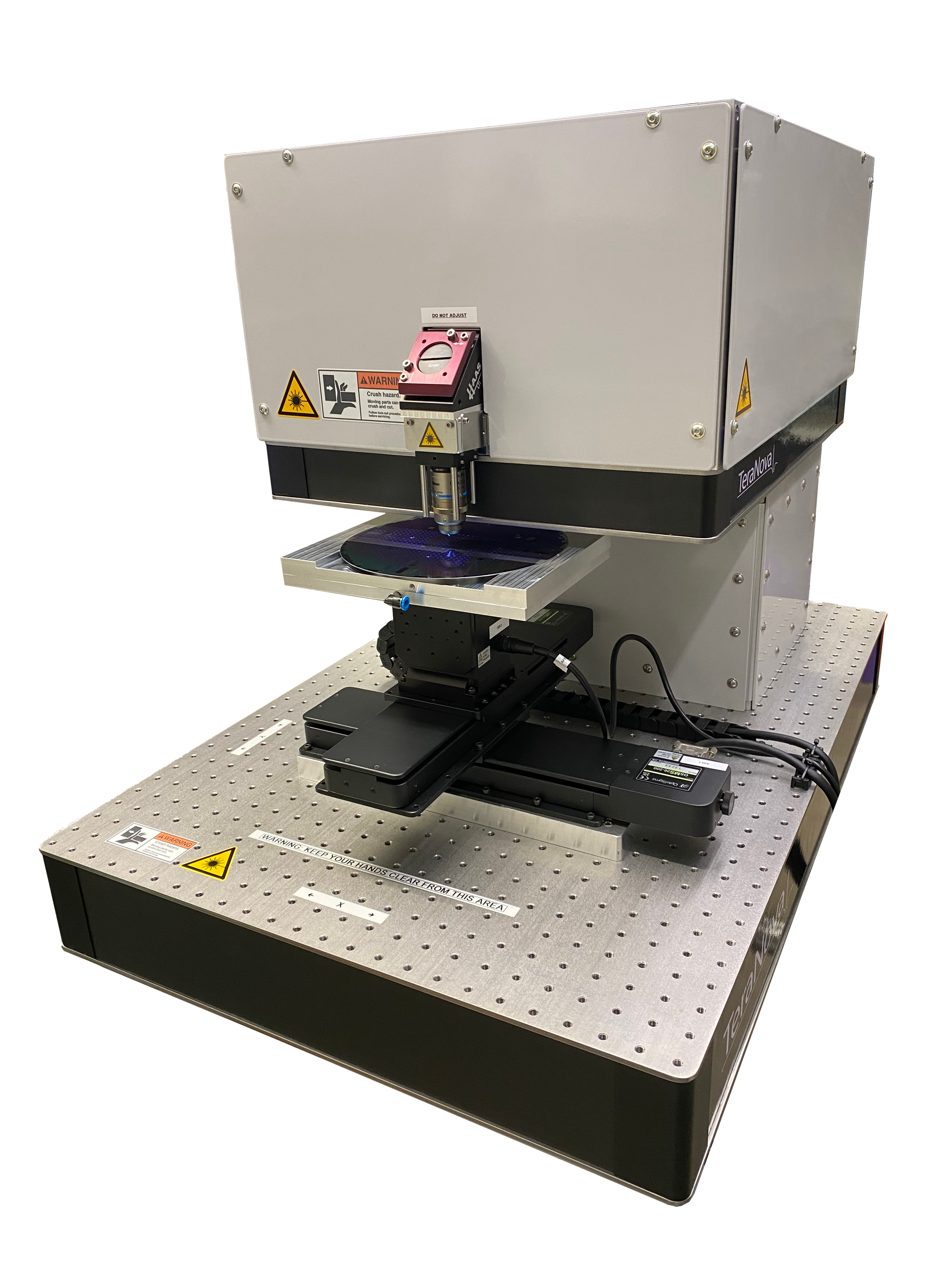
TeraNova, a start-up based in Eindhoven, addresses this need with its patented technology for in-line, non-destructive quality inspection of nanostructures and the estimation of their geometrical parameters. This technology measures the scattering properties of laser light from the nanostructures and analyses the resulting signals to accurately determine their geometrical characteristics. However, analysing these signals is computationally intensive. To perform real-time inspections over large production volumes, leveraging high-performance computing (HPC) is essential. In this project, TeraNova will collaborate with 81Watts to develop the necessary HPC infrastructure for real-time quality inspection of photonic nanostructures, addressing a critical need in the market.
Organisations involved:
End User: TeraNova BV
ISV, Domain expert, HPC provider, Technology expert: 81Watts